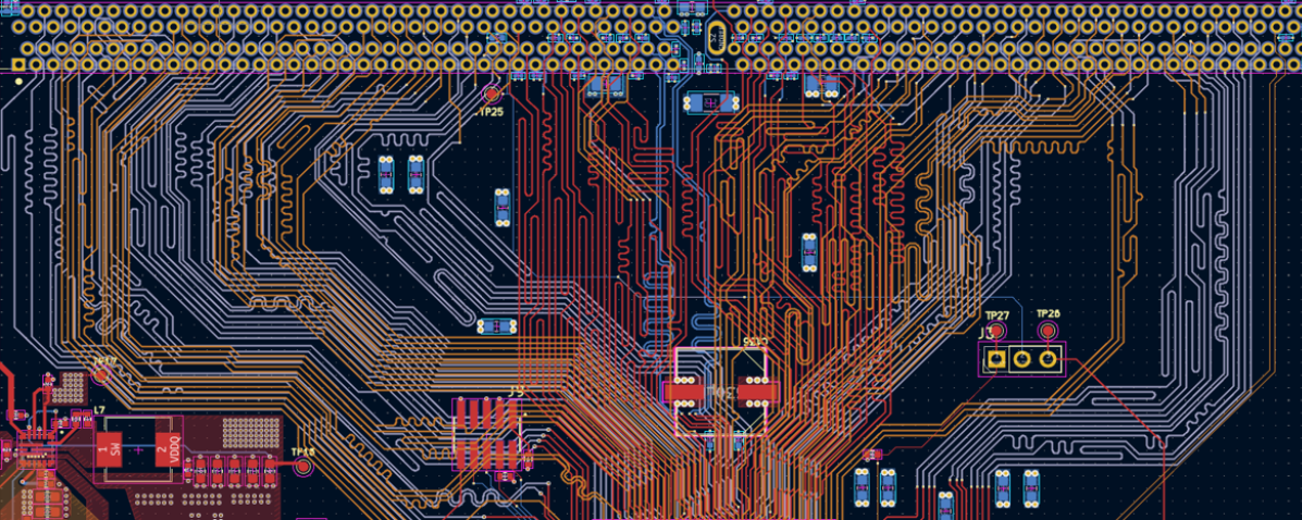
Termination, Reflections, and Signal Integrity: Foundations
Most embedded computing systems use some form of high-speed logic signal. Whether it be a memory interface such as DDR4, a communication bus like PCIe, or even USB, these signals must be terminated to work properly and avoid reflections. Reflections contribute to all sorts of signal integrity issues. The effects of these issues could be severe performance degradation, non-functionality of the system, or even damage to components. Termination means adding some sort of hardware component to absorb electromagnetic energy in the signal at the right time.
Why and When to Terminate
A common misconception when it comes to signal termination is that only high-frequency signals need to be terminated. This is untrue. Even a signal that only switches once per millennium might need to be terminated for proper operation.
Why
What causes a signal to be considered "high-speed" is not its frequency. Whether or not a signal is high-speed depends on the combination of its edge rates (rise and fall times expressed in slew rate or volts per second) and the length of the line that it is connected to. To understand why to terminate, we first need to examine the physics of transmission lines.
In short, a wire appears as a transmission line to high-frequency signals. The exact behavior of the transmission line is dependent on the wavelength of the electromagnetic wave passing through it. But wait, you might say – we just said that even low frequency signals might need to be terminated. This is still true. When a signal switches, regardless of its base frequency, that rising or falling edge has constituent high-frequency harmonic waveforms that can be revealed with a Fourier transform. Without delving too deep into the mathematics, the sharper the transition, the more high-frequency components are involved. It is a fundamental property of signal theory and Fourier analysis. These constituent high-frequency components are what is interacting with the transmission line.
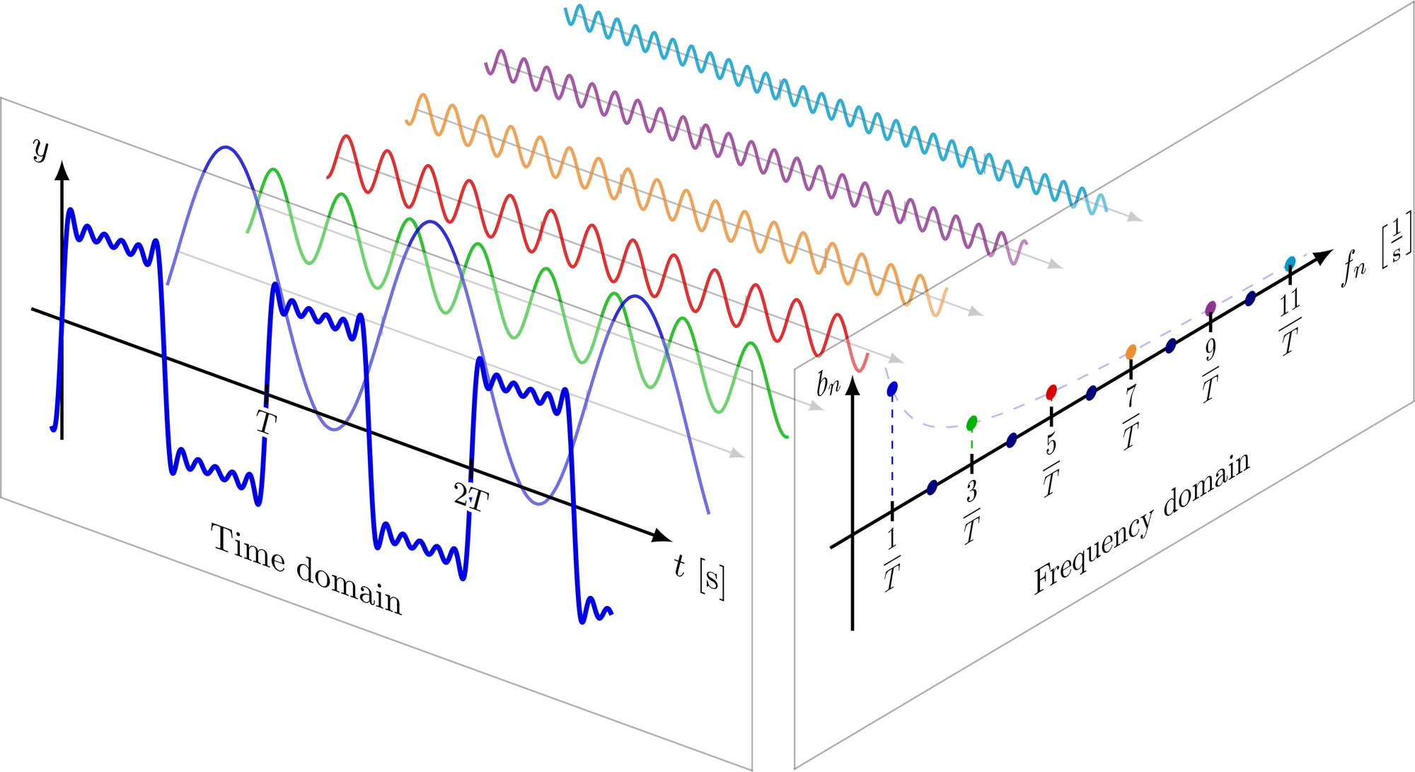
Electromagnetic fields propagate through PCB traces at a speed dependent on the dielectric material of the PCB. For most purposes, it is 6 inches per nanosecond. Transmission line effects become significant when the length of the line is a substantial fraction of the wavelength of the signal's high-frequency components. If this is the case, signal integrity issues can arise due to the high-frequency components interacting with the transmission line, such as reflections due to impedance changes in the line. However, if the length of the line is short enough compared to the signal's wavelength, these high-frequency components do not have enough time to establish standing waves or reflections before the voltage settles. In this case, the driver, transmission line, and receiver can be treated as a lumped circuit and termination is not necessary.
When
Knowing that EM fields propagate through a PCB trace at 6 inches per nanosecond, it is helpful to think of edge rates as the distance that an EM field could travel in that time. This is known as the electrical length of a signal. For example, if a signal has an edge rate of 1 ns, its electrical length is 1*6=6 inches. As a rule of thumb, if the length of a PCB trace is greater than 1/4 the electrical length of the signal's edge rate, it is considered high-speed and must be terminated.
It is now easy to see how the misconception that only high-frequency signals need to be terminated arose. As switching frequency increases, its switching slew rate must increase too because there is less time for it to do so within a cycle, which necessitates termination. As an example, DDR4 data signals can switch in as little as 150 picoseconds. The corresponding 1/4 electrical length is only 225 mils! It would be a massive challenge to route all of those signals with the DRAM chips so close to the controller. The natural solution is to terminate them instead.
Reflections
We are talking about impedance, not resistance, because of the high-frequency components present. The system as a whole must be examined from an AC circuit analysis standpoint. We are not dealing with direct currents.
PCB traces and input pins have parasitic capacitance. This capacitance is what a signal's EM field is charging to induce voltage on the transmission line or pin. Combined with parasitic inductance, it is also what causes transmission lines to have their characteristic impedance. A "load" for a logic signal is usually the receiver's input parasitic capacitance, which is very small and absorbs a negligible amount of the EM field's energy. The load input impedance can also be considered infinity (in actuality, usually >10MΩ).
Trace Impedance
Conductors on a PCB have a characteristic impedance. This characteristic impedance is not cumulative and is dependent on many things: trace geometry (width, thickness, shape), dielectric material (the quantity of most importance is the dielectric constant – higher means more capacitance per unit length, thus lower impedance), dielectric thickness, reference planes (closer means more capacitance, and splits or slots in the reference plane disrupt return paths, increasing impedance), stackup, coupling to nearby conductors, etc. These things all contribute to the trace's parasitic capacitance and inductance per unit length. This is why, for critical applications, controlled impedance is necessary.
Characteristic impedance does not scale with length because it is determined by the ratio of the trace's inductance and capacitance per unit length. High-frequency waves travelling along such a transmission line do not "see" or interact with the total capacitance or inductance at once. It propagates along the trace, interacting with distributed inductance and capacitance as it moves. This is modeled as a distributed network. You can think of a trace carrying high-frequency waves as like an infinite series of tiny LC sections. The impedance at each "step" is local and governs how energy is transferred at that point (voltage resulting from current). So, a change in this characteristic impedance is going to cause a change in energy transfer along the line. This is what we are interested in. However, as discussed previously, if the line is electrically insignificant (much shorter than the signal's wavelength), the lumped inductance and capacitance is seen all at once, not a distributed network. The signal does not have time to fully propagate and build up the distributed behavior. There is no significant delay in propagation across the trace, so voltage and current rise nearly simultaneously everywhere along it, thus the conductor can be treated as a lumped circuit (a single small capacitor or inductor).
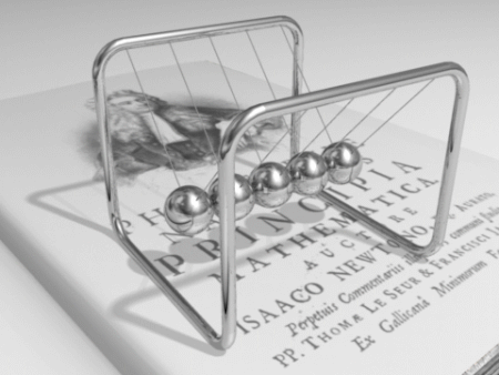
Reflections occur when there is a change in impedance on a transmission line. When the EM field encounters a change, some or all of its energy will be reflected in the opposite direction, back down the transmission line. The magnitude and sign of the reflection depends on the difference between the upstream and downstream impedance. If an EM field encounters a load such as a receiver's input pin, it effectively sees an open circuit due to the very high input impedance. In this case, all of its energy is reflected back down the transmission line. A helpful visualization for this is Newton's Cradle. In effect, the exact same physical process is happening.
The effect of such a reflection is to charge the capacitance to double the voltage that it was already charged to by the initial launching of the EM field. As the reflection travels back down the transmission line, every point along it is charged to double what it already was. It is easy to see how this can cause problems.
Termination
Series Termination
The magnitude of the initial EM field that is launched onto a transmission line is called the bench voltage. Bench voltage is a result of the voltage divider formed by the driver's output impedance and the line impedance. It is given by the equation Vbench = (Zline / (Zline+Zout) * Vlogic.
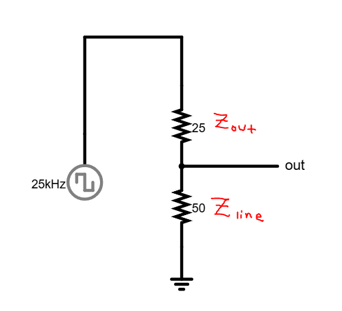
If Zout and Zline are exactly equal, Vbench is half of the logic voltage. This is what we want. Remember, when the wave reflects due to an open circuit (or extremely high input impedance), voltage will double. If the initial voltage is half of what we want, when it doubles, we will have exactly the correct voltage.
The problem is that these two impedances are never equal by default. There are two main factors at play here. Firstly, if the PCB traces are not impedance controlled, it is impossible for the design engineer to know exactly what the line impedance will be anyway (PCB stackups and impedance controlling can be an entire blog post on its own). Secondly, the output impedance of the logic driver varies between logic family and specific chip.
Thankfully, Zout is usually less than Zline, which means that we can do something to bring it up to Zline. If we know Zout (which be obtained through component datasheets or SPICE modeling), we can simply add a resistor in series with the driver to bring Zout up to Zline. The value that we want is given by the equation Zst = Zline - Zout. This is called a series termination. When the reflected wave arrives back at the driver, if the impedances are matched, another reflection will not occur (remember, reflections occur when impedance changes) and all of the EM field's energy will be absorbed.
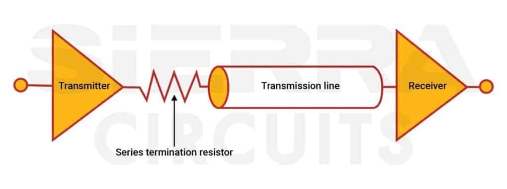
There is one massive downside to series terminations. In a series-terminated circuit, we are actually relying on the reflection for proper operation. As a result, the speed at which the signal can switch for a given trace length becomes severely limited. Logic levels are only valid on the line after the reflection reaches the point where it is sampled and the voltage doubles. The only point with logic levels that are always valid is the furthest load end where the wave reflects; if any other devices are on the same line, they must wait for the reflected wave to reach before their data becomes valid. This puts us in much the same situation as if we didn't terminate at all. To get faster speeds, we have to decrease the distance, which is only feasible up to a point.
Parallel Termination
A solution exists. Instead of using a series termination and relying on the reflected wave to bring the voltage up to what we want, we can simply place a resistor in parallel at the load end of the line. The value of this resistor must be matched to the impedance of the line so that it can properly absorb the EM field's energy once it reaches the resistor. In this case, there is no reflection. The EM field is completely absorbed at the load end.
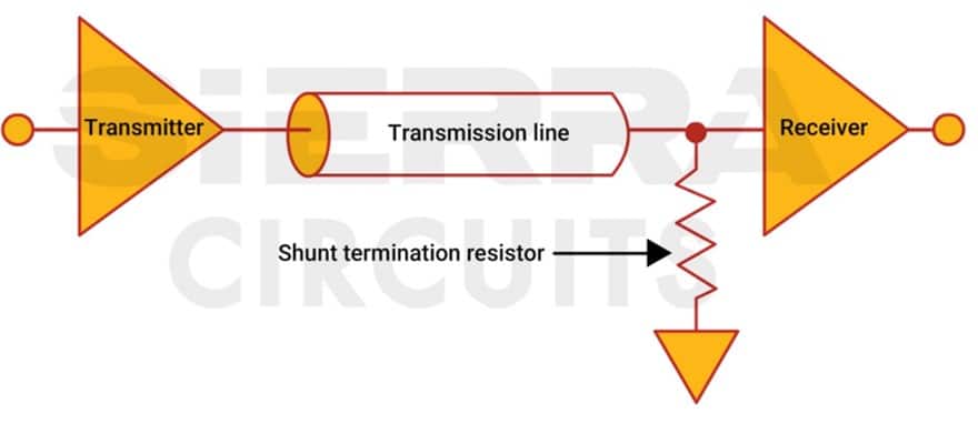
Usually, the output impedance for drivers intending to be parallel terminated must be very low. Since there is no reflection, voltage doubling cannot be relied on to get the proper logic level. If the bench voltage is half that of the logic voltage, as in series termination, we would never have valid logic levels. To compensate, we can lower the output impedance of the driver. Going back to the Vbench equation from earlier, we can see that a lower output impedance means higher Vbench for a given line impedance. Ideally, Vbench should be as close as possible to the logic voltage, which means the output impedance must approach 0.
No reflection means that a valid logic level exists across the entire line as soon as the initial EM field passes through. The result is no dead time where devices have to wait for a reflected wave, meaning the line can switch much faster and still be valid.
The drawback is power consumption. For a typical line impedance of 50Ω, current draw can be as much as 3.3/50 = 66mA for 3.3v logic. For a lot of applications, this is unacceptable. To solve this problem, logic families using parallel termination operate at a much lower voltage. For example, the voltage swing for LVDS signals is only 400 mV. At lower voltage, however, noise becomes a greater concern because there is less margin of error. Parallel terminated lines must be much more carefully isolated from noise than other termination schemes as a result.
Practical Systems and Termination Voltage
Differential Signaling: Theory
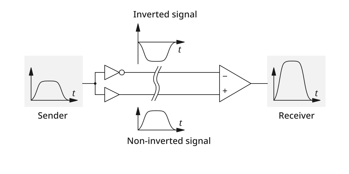
Most systems that utilize signal termination are differential. Differential signaling relies on retaining symmetry between the two driven lines. In differential signaling, the transmitted data is represented by the voltage difference between the two signal lines, as opposed to single-ended signaling that transmits based on the absolute voltage of the line relative to ground. Differential receivers decode the signal by subtracting one line from the other, which inherently rejects noise that affects both lines equally (common-mode noise). Differential signaling is also immune to ground bounce.
Differential signals are centered around a common-mode voltage. The common-mode voltage is the average voltage shared by the two signal lines. It is the component of the signal that is common to both lines in a pair, rather than the difference between them. In mathematical terms, it is expressed by the equation Vcm = (V- + V+) / 2. The common-mode voltage is therefore the baseline around which the differential signal swings. In practical systems, it is deliberately set to a value above 0v to avoid having to use a dual voltage supply. If the common-mode voltage were 0v, it is implied that each signal line would eventually have to be driven to a negative value, which is not possible in most electronic systems that operate only on a positive supply. For example, a system in which one line swings from 1.4 to 1.0v and the other from 1.0 to 1.4v, has a voltage swing of only 400mV and a common-mode voltage of (1 + 1.4) / 2 = 1.2v.
Termination Voltage
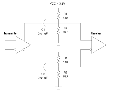
In the above discussion on parallel termination, one could infer that the termination resistor is always connected to ground. In practice, this is rarely the case. For most differential signals, the termination voltage (Vtt) is matched to the ideal common-mode voltage of the differential signals.
One of the primary reasons for matching Vtt to the common-mode voltage is to minimize power consumption. When the termination voltage matches the common-mode voltage, the DC bias of the line aligns with the natural balance of the differential signal. This minimizes current flow through the termination resistor, since there is no path for current to flow on average (current will not flow from 1.2v to 1.2v). So, power consumption is minimum except for dynamic signal currents. For example, a system using 1.2v common-mode voltage and 400mV swing has a maximum voltage of 1.4v. The resulting current draw at the top of the swing and termination impedance of 50Ω is (1.4-1.2) / 50 = 4mA. Since this is true for both lines, the total current draw just becomes the voltage swing divided by termination impedance. In this case, 0.4/50 = 8mA. So, when using differential signaling, setting Vtt to the ideal common-mode voltage is required.
It is also important to match Vtt to the common-mode voltage in order to ensure signal integrity. If it differs from the common-mode voltage, the termination network can introduce unintended bias that can disrupt the balance of the differential signal. This can negatively impact the symmetry of the differential signals, which reduces the receiver's ability to reject common-mode noise. A mismatch between Vtt and common-mode voltage can also introduce an impedance change at the termination point due to current flowing from the inaccurate DC bias.
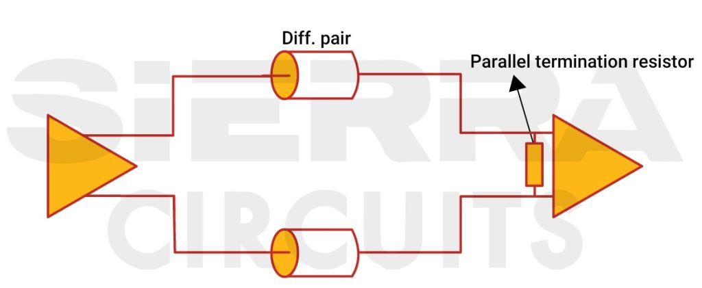
When using differential signals, the most common termination method is differential termination. In short, a resistor equal to the value of the differential impedance is placed between the two lines (an explanation of differential impedance is outside the scope of this post). This is very similar to parallel termination. In this scheme, the resistor does not impose any external bias to the lines. The termination voltage naturally remains centered at the common-mode voltage. The advantage of this technique is simplicity, since only one resistor is needed and no external voltage level is required.
Given these considerations, it is important that the copper plane on the PCB supplying the termination voltage (if applicable) is solid, properly decoupled, and isolated from noise. When data is being transmitted over multiple differential pairs at once (as is the case in many protocols such as DDR4 and PCIe), a large amount of power can be dissipated through the termination resistors. Bulk capacitance is therefore also necessary to supply transient power needs in the low frequencies. Any noise or voltage fluctuations present on Vtt can directly affect the signal integrity of the system.
AC and DC Coupling
All of this assumes that the differential transmitter's common-mode voltage falls within the receiver's acceptable range. If this is the case, then no other circuitry is required and the signal is said to be DC coupled. This would be the case when using an LVDS transmitter and an LVDS receiver, for example.
However, in a lot of cases, your transmitter is using a different logic family than the receiver. This often means that the transmitted common-mode voltage is different than what the receiver expects, which will lead to failures in interpreting logic high and logic low on the differential line. This can be fixed with a technique known as AC coupling.
In AC coupling, a capacitor is placed in series on each line. The capacitor serves to block the DC component of the signal, allowing only the AC waveform (used for timing) through. Once the DC component is removed, the signal will no longer have the proper DC bias. A DC restore circuit is therefore required to set the common-mode voltage to the expected level before it reaches the receiver. This is typically built into many receivers, but if not, it can be accomplished with a simple resistor divider. So, AC coupling with a DC restore circuit essentially corrects the common-mode voltage so that the differential signal swings around the voltage that the receiver expects. A typical choice for AC coupling capacitors is 0.01 μF, in the smallest package possible.
AC coupling also reduces power consumption by blocking any DC current between the transmitter and receiver. If the common-mode voltage of the transmitter does not match the receiver's expected input level, a DC offset is created, so there is static DC current. Even when there is no AC swing, DC current can exist, that AC coupling capacitors block.
The resulting circuit (between the capacitor and termination resistance) is a simple RC high-pass filter. Therefore, the value of the AC coupling capacitor should be chosen for the correct cutoff frequency, typically much less than the signal's fundamental frequency to avoid attenuating it. If the capacitance is too small, it can attenuate the low-frequency components of the desired signal, distorting it. If it is too large, the time to charge/discharge will be too high and the signal will be slowed down.
Final Remarks
Other termination schemes exist. In fact, the exact termination scheme that you should use depends on the I/O family. The relevant standards or documentation should be consulted. This post was a brief overview of why termination is necessary and the most commonly used techniques.
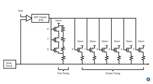
A lot of chips designed for high-speed operation also have configurable On-Die Termination (ODT). Most FPGAs, microprocessors, and DRAM chips have this option. With ODT, the termination resistor is built into the device. This reduces the need for external resistors, which saves cost and PCB density.
With all of this information in mind, it should be easier to make informed decisions about signal integrity when designing hardware for high-speed computing systems or logic in general.