Power Delivery Networks for High-Performance Circuit Boards
Note: this article assumes a foundational knowledge of AC circuits. My previous article introduces important topics such as reactance, frequency vs. impedance, and resonance. This article is more about theory and applications than math since it is assumed that the reader already understands the math and underlying concepts. I highly recommend reading that article first, since we build on the topics introduced there in this article.
I. Introduction: The Critical Role of PDNs
When it comes to high-performance electronics, the Power Delivery Network (PDN) is one of the most important and often overlooked aspects. At its core, a PDN is responsible for delivering stable power to components such as processors, FPGAs, and memory modules – no stable power means no stable operation. Yet, designing an effective PDN is far from straightforward and requires a strong knowledge of AC circuits. Poor PDN design can lead to costly complications such as excessive radiated emissions or bad noise immunity, causing designs to fail certification.
To understand the importance of PDNs, consider the strict voltage ripple tolerances outlined in FPGA, microprocessor, and memory datasheets. These components tend to be very sensitive to noise. For instance, an FPGA's core voltage may operate within a range of ±50 mV, with even minor deviations leading to performance degradation or system instability. When dealing with gigabit transceivers, the margins get even tighter. Xilinx recommends less than 10 mV peak-to-peak noise at point of load from 10 kHz all the way to 80 MHz for 7-series gigabit transceivers.
"High-performance" is a purposefully vague term. It could refer to high clock speeds, data rates, or power in general. In today's world, we are surrounded by and rely on high-performance circuits for connectivity and processing. Understanding the importance of power delivery in these systems is crucial. So, given the importance and requirements, what can we do to design effective PDNs?
II. Fundamental PDN Concepts
A well-designed PDN is necessary for most electronic devices because they tend to have unstable power demands. Since voltage is fixed, a change in power consumption means a change in current. For most processors and FPGA designs, current demand fluctuates based on what the device is doing – a state change can easily induce a spike or dip in current draw. These changes can happen in times ranging from days to picoseconds. The goal of a PDN is to deliver stable voltage to electronic components under all operating current demands.
Noise Sources and Frequency
The variance in current demanded by a digital device occurs at low and high frequencies. The PDN therefore must be able to maintain voltage stability across a wide bandwidth. Low-frequency current draw changes are the result of individual devices being enabled or disabled, such as waking up microprocessors or enabling memory chips. High-frequency changes are the result of switching within devices, scaled by the clock frequency. In general, the higher the clock frequency, the higher the bandwidth the PDN must be able to regulate power at.
Noise can also be induced into the PDN from external sources, such as noise from switching regulators, coupling from other nearby circuits, or radiated emissions from other devices. The amount of noise introduced by these sources depends heavily on current loop areas present in the PCB.
Power Delivery
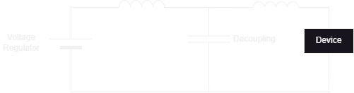
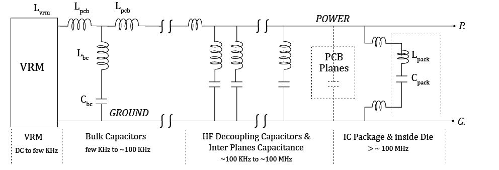
The component of a PDN that is able to supply DC power is the voltage regulator. A regulator uses a feedback loop to adjust its output current to keep the output voltage constant. It can only do this so fast. For lower frequencies (a few hundred kilohertz), the regulator can be relied on to maintain a constant output voltage. However, for transients at higher frequencies, it cannot respond immediately and thus its output voltage varies for some time until it can.
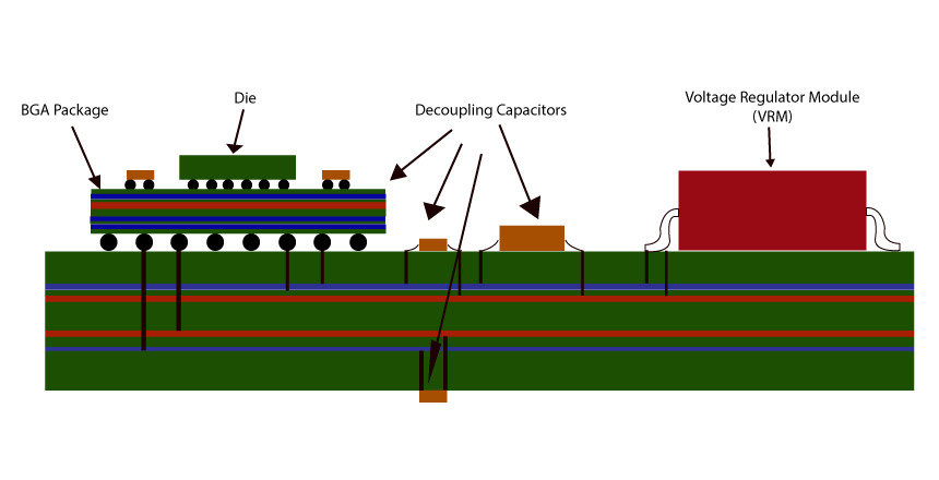
Decoupling capacitors make up for the lost time. They work as local energy storage for the device and can respond much quicker to changing current demands, maintaining power supply voltage at frequencies up to hundreds of megahertz. Their effective frequency will be examined in detail in a later section. These capacitors work in parallel with the voltage regulator, with some amount of parasitic inductance between.
Inductance and Impedance
In an ideal world, none of this would matter because there would be no parasitics and the PDN would maintain 0 impedance, providing a perfect voltage with no change as current changes. Unfortunately for us, we live in the real world and so the PDN has parasitics, and thus, unintended impedance. Voltage develops across this impedance as current flows through it, manifesting as noise or voltage drop (by V = IZ).
Parasitic inductance exists at all stages of the PDN, in all current paths. When current flows through any conductor, a magnetic field is generated and energy is stored in it (by Ampere's law), creating inductance. Inductance resists change in current, so it decreases the ability of capacitors and regulators to supply power during transient current changes. This can be modeled as impedance, or the general opposition to time-varying current flow. For a fixed frequency, increasing inductance increases impedance. As impedance increases, transient response from regulators and capacitors slows and observed noise increases.
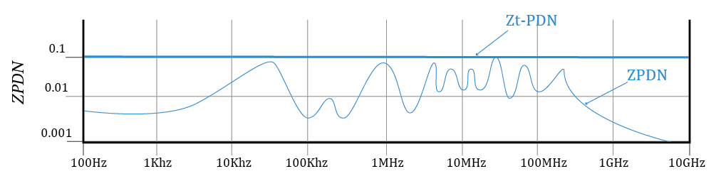
As we've already described, current demand can change in times ranging from picoseconds to days. Lower inductance means lower impedance regardless of frequency, so steps should be taken to decrease parasitic inductance wherever possible. The goal of a PDN is a low, flat impedance curve over the entire spectrum of operating frequencies. Ideally, there should be no peaks, meaning the PDN should be able to supply current without relative voltage dips or spikes at all frequencies. Now that we've described how a PDN works and identified the challenges and goals, how do we make sure a PDN has low impedance across a wide bandwidth?
III. Capacitance in PDNs
Capacitors are some of the most important aspects of PDNs and help solve many problems. By providing energy storage and filtering noise, they ensure that transient current demands are met quickly and they play a critical role in stabilizing wideband power. They fall into two main categories in the context of PDNs: bulk and decoupling.
Bulk Capacitors
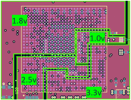
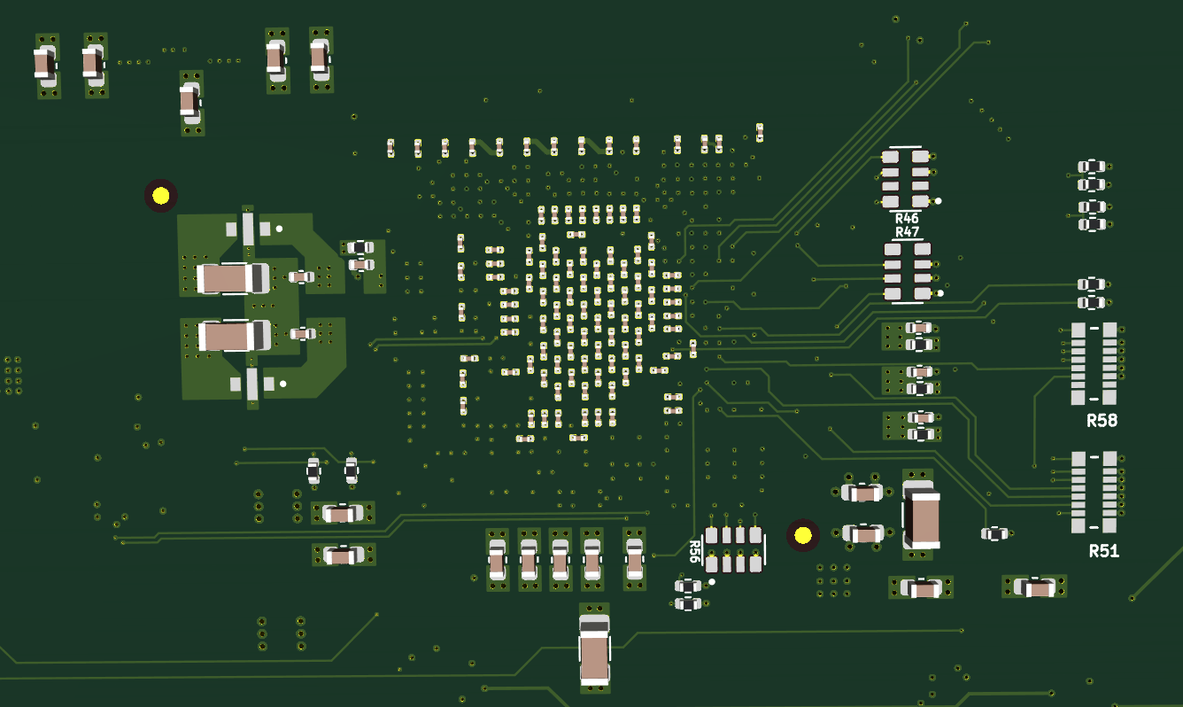
Bulk capacitors are larger-value capacitors that are distributed throughout the PCB. Their primary function is to provide energy storage to stabilize entire planes and respond to low-frequency transient current demands. The exact placement of bulk capacitors is not critical because there is more time margin for the energy to propagate through PCB dielectric at low frequencies. However, proximity to the load is still preferred. They should be distributed around the PCB and not clustered in one area so that every point of load for a given voltage is not too far away from a bulk capacitor and has adequate low-frequency response.
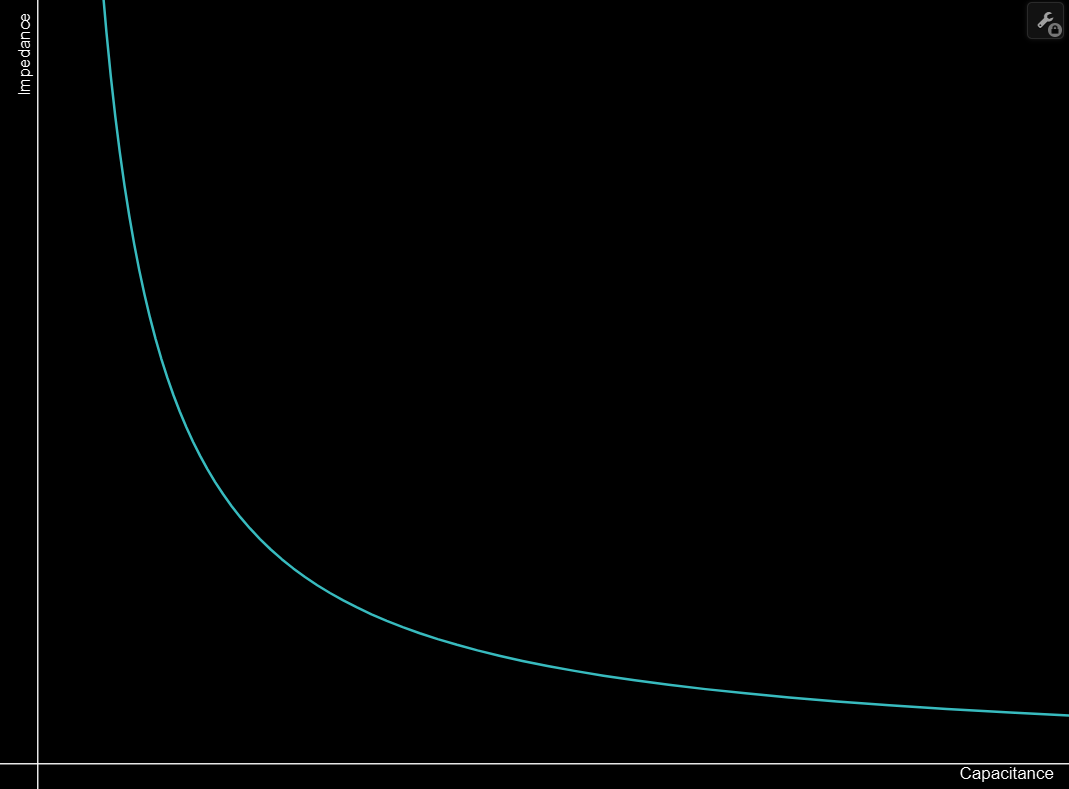
As Figure 6 shows, at a fixed frequency, impedance decreases with increasing capacitance. This is why bulk capacitors are higher in value; when frequency is low, you want to increase capacitance as much as possible to maintain low impedance. Bulk capacitors can be thought of as fast-acting energy sources that can respond to changes in current demand faster than the regulator can, but slower than decoupling capacitors.
Decoupling Capacitors
Decoupling capacitors are smaller-value, smaller-package capacitors that are located as close as possible to the point of load. They provide energy that can respond to the load's transient current demand in the high frequencies and smooth out voltage fluctuations caused by rapid switching within components. They also provide a path for high-frequency noise, filtering it before it reaches the load point. Their performance in a PDN depends heavily on their mounting location and self-resonant frequency (SRF).
Decoupling capacitors should be placed as close as possible to the point of load to decrease current path inductance and time delay before energy can transfer from the capacitor to load pin (typically through FR4 dielectric). Generally, you want at least one decoupling capacitor per power pin.
To decrease high-frequency impedance, inductance can be lowered, but that is usually not possible for a given package size. However, using multiple capacitors in parallel can decrease the inductance. Paralleling multiple capacitors therefore lowers both high frequency and low frequency impedance at the same time, since you're increasing capacitance and lowering inductance at the same time. Many critical applications call for multiple decoupling capacitors per pin for this reason.
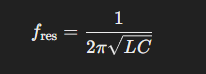
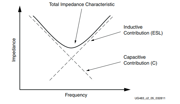
A real capacitor forms a series RLC circuit comprised of its capacitance, equivalent series resistance (ESR), equivalent series inductance (ESL), and mounting inductance. For effective decoupling, the mounting inductance should be lowered as much as possible by using short and wide traces, via-in-pad, and small package sizes. Referring to Equation 1, it is easy to see why decoupling capacitors are smaller-value: the smaller the capacitance for a given inductance (ESL and mounting), the larger the SRF.
Self-Resonant Frequency
Real-world capacitors are not perfect; they behave as series RLC circuits with capacitance. Therefore, as with any series RLC circuit, they have a resonant frequency that corresponds to the lowest impedance. This is called the capacitor's self-resonant frequency. When choosing decoupling capacitors for a specific application, its SRF should be considered with as much importance as the value of capacitance.
At their self-resonant frequency, the impedance is at a minimum, making it highly effective at filtering noise and supplying transient current. Beyond this frequency, the inductive component dominates and reduces the effectiveness. In general, for a given capacitance value, the smallest package should be chosen to minimize inductance and maximize SRF. The SRF, and thus, capacitor, for a specific decoupling application should be carefully chosen. Capacitors are most effective for decoupling purposes at their SRF; outside of that narrow band, they are less effective and don't contribute much to the PDN.
Combination of Capacitors
We've examined the different types of capacitors and their roles in a PDN. But how do you actually use them? For optimal PDN performance, and to accomplish the goal of a PDN having a flat impedance curve over a wide frequency bandwidth, multiple capacitors with varying values should be used. This approach ensures that the PDN maintains low impedance across the necessary spectrum, providing effective filtering and transient supply at key frequencies.
It is most important to choose multiple decoupling capacitors due to their higher effective frequency. Choosing multiple different values means that you have multiple self-resonant frequencies, so the PDN's total impedance characteristic curve forms "valleys" at these frequencies as impedance dips.
These valleys should exist at key frequencies, such as the main clock frequency and its harmonics. Component datasheets should be consulted to assess the range of frequencies over which current transients should be expected during different programmed states for your application. The output impedance of the voltage regulator determines the low-frequency boundary (typically a few hundred kHz), as capacitors must take over decoupling above this range. Capacitor values should provide low impedance at overlapping frequencies. For example, large-value capacitors for <1Mhz, medium-value for 1-100MHz, and small-value for >100MHz.
Q-Factor
Every capacitor has a Q-factor that determines the shape of its impedance characteristic (refer to Figure 7). A lower Q-factor means that the curve is flattened, which is ideal, because that means it can be effective for a wider range of frequency centered around its resonant point. However, most ceramic decoupling capacitors have a low ESR. Lower series resistance means higher Q-factor, making it even more important to have multiple capacitance values to cover a broad frequency spectrum for decoupling. Q-factor can be lowered by damping the RLC circuit with added resistance, but a better option is to add capacitors with higher ESR (such as bulk tantalum or electrolytic capacitors).
IV. Minimizing Inductance
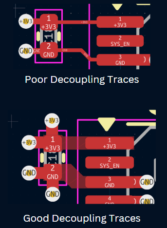
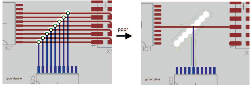
The parasitic inductance in the PDN comes from device mounting (leads, pads, and solder) and PCB power planes. The inductance that a given current path experiences is proportional to its loop area; therefore, it is important to minimize all loop sizes by using short traces and a minimal amount of vias. Current flows from a regulator to the device and back to ground, traveling through power planes, vias, and solder lands.
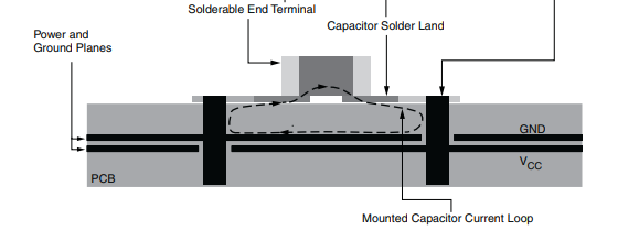
Connecting trace lengths should be as wide and short as possible to minimize inductance. The best option is to not use connecting traces at all, but to use via-in-pad to place the via directly in the pad. In general, wider traces with less change in direction and shape contribute less parasitic inductance. Inductance in planes is a function of the shape, not the size, since current spreads as it flows.
Minimizing inductance minimizes impedance and maximizes the frequency response of decoupling capacitors. For effective wideband filtering, these techniques should be followed wherever possible.
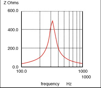
V. Anti-Resonance
While the goal of a PDN is to achieve a flat, low-impedance characteristic across a wide frequency range, a significant challenge arises in the form of anti-resonance. Anti-resonance is a phenomenon where parallel RLC circuits within the PDN create high-impedance peaks at certain frequencies (the opposite of the valleys we create with decoupling capacitors), resulting in poor transient response and increased noise susceptibility.
What Causes Anti-Resonance?
Anti-resonance occurs when the impedance of two or more parallel capacitors interacts with the parasitic inductance of the PCB power planes or traces. Instead of reinforcing low impedance, this interaction creates frequencies where the impedance spikes. This can have several detrimental and often catastrophic effects at these frequencies. Just as the impedance of a series RLC circuit is minimum at resonance, the impedance of a parallel RLC circuit is maximum at resonance.
Minimizing Anti-Resonance
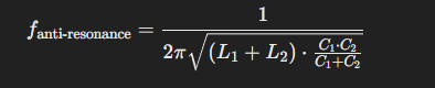
If the load has a transient current demand at anti-resonant frequencies, large noise voltages can occur because impedance is high and the PDN cannot quickly respond to the change in current draw. To minimize the effect of anti-resonance, multiple capacitor values should be used. This spreads the anti-resonant peaks over a wide frequency range instead of being amplified at certain frequencies. The anti-resonant point of parallel capacitors with parasitic inductance can be found with the following formula:
The impedance curve could also be flattened by introducing higher ESR capacitors to lower the overall Q-factor, which will reduce the height of anti-resonant impedance spikes. Alternatively, discrete damping resistors can be placed in series with certain resistors to accomplish the same thing (which would work well for specific troublesome frequencies that you wish to damp). Power plane design should be optimized to be uninterrupted and uniform to reduce parasitic inductance that contributes to anti-resonance.
It may be possible to combat anti-resonance in software instead of spinning new boards. If a state change causes transient current demands at an anti-resonant frequency, something could be tweaked in software (a clock scaler, timer, frequency, etc) to shift the current demand out of anti-resonant territory.
VI. Current Loops
Current loops play a critical role in determining the effectiveness of a PDN and the overall electromagnetic compatibility (EMC) of the system. Improperly managed current loops can lead to increased electromagnetic interference (EMI), signal integrity issues, and power distribution problems.
Current Loops in PDNs
A current loop is formed whenever current flows from a source (e.g., the power supply) to a load (e.g., a processor) and returns back to the source. The area enclosed by this loops is directly related to EMI and inductance. The larger the loop area, the greater the magnetic field generated. This magnetic field can radiate energy as EMI (especially problematic for high-frequency signals), potentially interfering with nearby circuits. It also increases the inductive reactance, increasing PDN impedance.
When current flows through a loop, it generates a magnetic field proportional to the loop area. At high frequencies, this magnetic field can radiate significant amounts of energy as EMI. This radiation can couple noise into nearby circuits, cause voltage drops in the PDN, and lead to regulatory compliance issues.
Large current loops can also increase the system's susceptibility to interference, causing external noise to be coupled into the system.
Grounding
Many designers do not consider the return path for power or signals. Solid, contiguous ground planes are extremely important. Ground planes should only be split under extreme circumstances (such as copper voiding under power inductors) and care should be taken not to slot them with vias.
When slots arise in the ground planes, the return current has to flow around the slot, taking a longer path back to source than it took to get to the load. This increases the loop area and radiated emissions, particularly if the signal is high-frequency. It also increases ground inductance which can lead to incompatible PDN impedance or ground bounce, causing signal integrity issues.
VII. Conclusion
This article provided a basic overview of Power Delivery Networks (PDNs) for high-performance circuit boards, covering concepts such as impedance management, capacitor selection, anti-resonance, and current loop optimization. While we’ve touched on the fundamentals, there’s much more to cover, including advanced topics like utilizing capacitance within PCB stackups (power to ground planes), optimizing power and ground plane layers, and choosing the right stackup configuration for specific applications.
I hope that this article amplifies the importance of an often overlooked portion of engineering high-performance digital systems. Understanding the topics in this article can help with all PCB design as well, not just high-performance embedded applications.